Here you go. Photos of the components around the charge input.
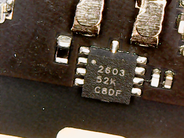
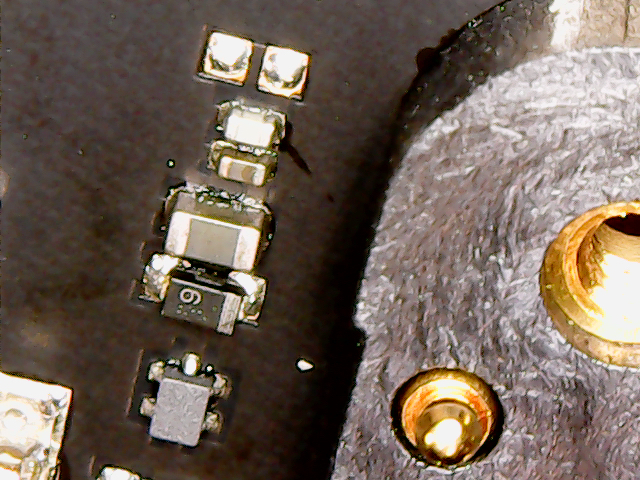
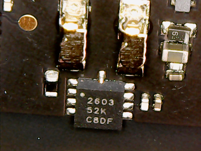
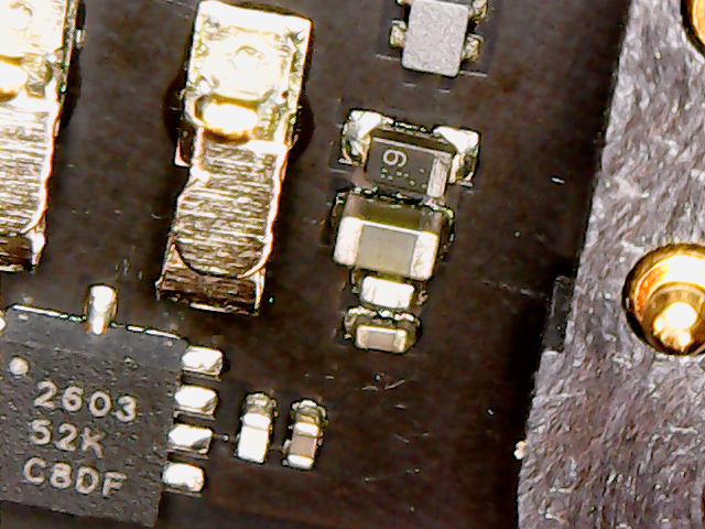
Here you go. Photos of the components around the charge input.


Can anyone make anything out of the pictures? What kind of chip could that be? Unfortunately you can not see any traces…
I read “2603 52k c8df” currently no clue. Power Manager? According to this list there are the following chip suppliers:
Taiwan Semiconductor (TSMC) 	 Integrated Circuits
FocalTech 	                 Integrated Circuits
Texas Instruments 	         Integrated Circuits
Synaptics 	                 Integrated Circuits
Skyworks 	                 Integrated Circuits
Samsung 	                 Integrated Circuits
RICOH 	                         Integrated Circuits
Qorvo 	                         Integrated Circuits
Qualcomm 	                 Integrated Circuits
Infineon 	                 Integrated Circuits
Fairchild 	                 Integrated Circuits
Maybe the list is incomplete or it’s not even an IC.
Yeah I can’t make cheese out of it either.
Maybe @keesj can enlighten us with some link to that part. Would be nice to
have some specs to know what we are dealing with.
Voltage stability (and thus need for decoupling) and voltage drop under
load characteristics would be extremely nice to have for power hungry or
sensitive applications.
The PCBs are pristine with internal tracks. Looked great, less useful for reverse engineering the circuit…
Is this cost efficient and really needed? I wonder, looks like overkill to me. It’s not all HF/IPC-2251 stuff. All I know is that they wanted to use ATS and “fair” gold.
Well it does make the phone safer against the non-engineers that will open it up.
Paul
Yup. But maybe there is a better reason for this. Just “ODM wanted it that way” would be kinda sad. Oh, and I just searched around a bit … I was not able to find something related to “2603 52k”.